- 您现在的位置:买卖IC网 > Sheet目录473 > MAX2839EVKIT+ (Maxim Integrated)KIT EVAL FOR MAX2839
�� �
�
�2.3GHz� to� 2.7GHz� MIMO� Wireless� Broadband�
�RF� Transceiver�
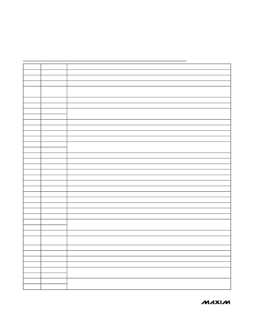
�Pin� Description�
�PIN�
�NAME�
�FUNCTION�
�1�
�2�
�GNDRXLNA_A� Receiver� A� LNA� Ground�
�VCCRXLNA_A� Receiver� A� LNA� Supply� Voltage.� Bypass� with� a� 22pF� capacitor� as� close� as� possible� to� the� pin.�
�3�
�4�
�B0�
�LOAD�
�Receiver� Gain-Control� Logic� Input� Bit� 0�
�Receiver� Gain� Select.� Positive� edge� trigger� latches� digital� gain� inputs� B0–B7� to� receive� A.� Negative�
�edge� trigger� latches� digital� gain� inputs� B0–B7� to� receive� B.�
�5�
�6�
�VCCRXLNA_B� Receiver� B� LNA� Supply� Voltage.� Bypass� with� a� 22pF� capacitor� as� close� as� possible� to� the� pin.�
�GNDRXLNA_B� Receiver� B� LNA� Ground�
�7�
�8�
�9�
�10�
�11�
�12�
�13�
�14�
�15�
�16�
�17�
�18�
�19�
�20�
�21�
�22�
�23�
�24�
�25�
�26�
�27�
�28�
�29�
�30�
�31�
�32�
�33�
�34�
�35�
�36�
�37�
�38�
�RXINB+�
�RXINB-�
�B4�
�B3�
�VCCTXPAD�
�B2�
�TXOUT+�
�TXOUT-�
�B1�
�B5�
�PABIAS�
�VCCTXMX�
�SCLK�
�ENABLE�
�CLKOUT�
�REFCLK�
�XTAL1�
�VCCXTAL�
�VCCCP�
�GNDCP�
�CPOUT+�
�CPOUT-�
�GNDVCO�
�VCOBYP�
�VCCVCO�
�CS�
�DOUT�
�DIN�
�RXBBIB-�
�RXBBIB+�
�RXBBQB-�
�RXBBQB+�
�Receiver� B� LNA� Differential� Input.� Input� is� internally� DC-coupled.�
�Receiver� and� Transmitter� Gain-Control� Logic� Input� Bit� 4�
�Receiver� and� Transmitter� Gain-Control� Logic� Input� Bit� 3�
�Supply Voltage for Transmitter PA Driver. Bypass with a 22pF capacitor as close as possible to the pin.�
�Receiver� and� Transmitter� Gain-Control� Logic� Input� Bit� 2�
�Power� Amplifier� Driver� Differential� Output.� The� pins� have� internal� AC� blocking� capacitors.�
�Receiver� and� Transmitter� Gain-Control� Logic� Input� Bit� 1�
�Receiver� and� Transmitter� Gain-Control� Logic� Input� Bit� 5�
�Transmit� External� PA� Bias� DAC� Output�
�Transmitter Upconverter Supply Voltage. Bypass with a 22pF capacitor as close as possible to the pin.�
�Serial-Clock� Logic� Input� of� 4-Wire� Serial� Interface�
�Transceiver� Enable�
�Reference� Clock� Buffer� Output�
�Crystal� or� Reference� Clock� Input.� AC-couple� a� crystal� or� a� reference� clock� to� this� analog� input.�
�XTAL� Input.� Connect� the� other� terminal� of� the� XTAL� to� this� pin.�
�Crystal� Oscillator� Supply� Voltage.� Bypass� with� a� 100nF� capacitor� as� close� as� possible� to� the� pin.�
�PLL� Charge-Pump� Supply� Voltage.� Bypass� with� a� 100nF� capacitor� as� close� as� possible� to� the� pin.�
�Charge-Pump� Circuit� Ground�
�Differential� Charge-Pump� Output.� Connect� the� frequency� synthesizer’s� loop� filter� between� these� pins�
�(see� the� Typical� Operating� Circuit� ).�
�VCO� Ground�
�On-Chip� VCO� Regulator� Output� Bypass.� Bypass� with� a� 1μF� capacitor� to� GND.� Do� not� connect� other�
�circuitry� to� this� pin.�
�VCO� Supply� Voltage.� Bypass� with� a� 22nF� capacitor� as� close� as� possible� to� the� pin.�
�Chip-Select� Logic� Input� of� 4-Wire� Serial� Interface�
�Data� Logic� Output� of� 4-Wire� Serial� Interface�
�Data� Logic� Input� of� 4-Wire� Serial� Interface�
�Receiver� B� Baseband� I-Channel� Differential� Outputs�
�Receiver� B� Baseband� Q-Channel� Differential� Outputs�
�18�
�______________________________________________________________________________________�
�发布紧急采购,3分钟左右您将得到回复。
相关PDF资料
MAX2851ITK+
TRANSMITTER MIMO 5GHZ 5CH 68TQFN
MAX2852ITK+
IC RECEIVER DFS 5GHZ 68TQFN
MAX2870EVKIT#
EVAL KIT MAX2870
MAX2904EVKIT
EVAL KIT
MAX3524EVKIT
EVAL KIT MAX3524
MAX3540EVKIT#
KIT FOR MAX3540 DVB TUNER
MAX3541EVKIT+
KIT FOR MAX3541 DVB TUNER
MAX3542CLM+
IC TV TUNER SGL CONV 48LFCGA
相关代理商/技术参数
MAX283X-RD0089
制造商:Maxim Integrated Products 功能描述:INTERFACE BOARD - Bulk
MAX2842ETN+
制造商:Maxim Integrated Products 功能描述:3.3-3.9GHZ MIMO WIMAX RF TRANSCEIVER - Rail/Tube
MAX2842ETN+T
制造商:Maxim Integrated Products 功能描述:3.3-3.9GHZ MIMO WIMAX RF TRANSCEIVER - Tape and Reel
MAX2850EVKIT+
制造商:Maxim Integrated Products 功能描述:EVKIT FOR MAX2850 - Boxed Product (Development Kits)
MAX2850ITK+
功能描述:射频发射器 5GHZ 4Ch MIMO Transmitter RoHS:否 制造商:Micrel 类型:ASK Transmitter 封装 / 箱体:SOT-23-6 工作频率:300 MHz to 450 MHz 封装:Reel
MAX2850ITK+T
功能描述:射频发射器 5GHZ 4Ch MIMO Transmitter RoHS:否 制造商:Micrel 类型:ASK Transmitter 封装 / 箱体:SOT-23-6 工作频率:300 MHz to 450 MHz 封装:Reel
MAX2851ITK+
功能描述:射频接收器 RF and RFID 射频接收器s - TRANSMITTER MIMO 5GHZ 5CH 68TQFN RoHS:否 制造商:Skyworks Solutions, Inc. 类型:GPS Receiver 封装 / 箱体:QFN-24 工作频率:4.092 MHz 工作电源电压:3.3 V 封装:Reel
MAX2851ITK+T
功能描述:射频接收器 RF and RFID 射频接收器s - TRANSMITTER MIMO 5GHZ 5CH 68TQFN RoHS:否 制造商:Skyworks Solutions, Inc. 类型:GPS Receiver 封装 / 箱体:QFN-24 工作频率:4.092 MHz 工作电源电压:3.3 V 封装:Reel